Copyright ©1995 by NeXT Computer, Inc. All Rights Reserved.
| E |
Details of the DSP
| Memory Map |
| The following table describes the memory map for the DSP private RAM (8K words). |
| Start | End | Name | |
| p:0 | p:$1FF | On-chip program RAM (`$' denotes hex) | |
| p:$2000 | p:$3FFF | Off-chip program RAM, image 1 | |
| p:$A000 | p:$BFFF | Off-chip program RAM, image 2 | |
| x:0 | x:$FF | On-chip data RAM, x bank | |
| x:$100 | x:$1FF | On-chip data ROM, x bank (Mu-Law, A-law tables) | |
| x:$2000 | x:$3FFF | Off-chip data RAM, x bank, image 1 | |
| x:$A000 | x:$AFFF | Off-chip data RAM, x bank, image 2 | |
| y:0 | y:$FF | On-chip data RAM, y bank | |
| y:$100 | y:$1FF | On-chip data ROM, y bank (Sine wave cycle) | |
| y:$2000 | y:$3FFF | Off-chip data RAM, y bank, image 1 | |
| y:$A000 | y:$AFFF | Off-chip data RAM, y bank, image 2 |
| Off-chip memory exists in two "images" for each space. In image 1, all three memory spaces occupy the same physical memory (in other words, the X/Y~, PS~, and DS~ pins of the DSP56001 are not connected when address line A15 is low). In image 2, x and y are split into separate 4K banks, and p overlays them both with an 8K image (that is, X/Y~ is used as address line A12 and PS~ and DS~ are not connected when A15 is high). External memory starts at 8K ($2000) instead of 512 ($200) because address line A13 in the DSP must be high to enable external DSP RAM. (Note that there is another enable for this RAM in the System Control Register 2.) |
| DSP D-15 Connector Pinouts |
| The following describes the output pins of the DSP D-15 connector at the back of the main unit. The left column is the connector pin number, and the right column is the signal name as it appears in the Motorola DSP56000/DSP56001 Digital Signal Processor User's Manual. |
| D-15 | DSP | |
| SCK | ||
| SRD | ||
| STD | ||
| SCLK | ||
| RXD | ||
| TXD | ||
| +12V, 500mA | ||
| GND | ||
| GND | ||
| GND | ||
| SC2 | ||
| SC1 | ||
| SC0 | ||
| GND |
| Figure E-1 shows the circuit through which signals are sent from the DSP to the D-15 connector. |
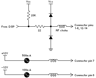 |
| Figure E-1. D-15 Connector
There's a series RF choke on each connector signal that doesn't affect its steady-state level. |
| DSP56001 Instruction Set Summary |
| The following notation is used in the summary: |
| Notation | Denotes | |
| `*' | Instructions that don't allow parallel data moves | |
| [a,b] | One of a or b | |
| <a,b> | Either a,b or b,a | |
| <n> | A nonnegative integer | |
| #I<n> | n-bit immediate value | |
| A<n> | n-bit absolute address | |
| An | A0, A1, or A2 (similarly for Bn) | |
| Xn | X0 or X1 (similarly for Yn) | |
| Rn | R0, R1, R2, R3, R4, R5, R6, or R7 (similarly for Nn, Mn) | |
| AnyEa | Addressing modes (Rn)[ | |
| AnyXY | [x,y]:AnyEa | |
| AnyIO | [x,y]:<<pp (x or y peripheral address, 6 bits, 1's extended) | |
| Creg | Registers Mn, SR, OMR, SP, SSH, SSL, LA, LC | |
| Dreg | Registers Xn, Yn, An, Bn, A, B | |
| Areg | Registers Rn, Nn | |
| AnyReg | Registers Dreg, Areg, Creg | |
| cc | CC(HS) CS(LO) EC EQ ES GE GT LC LE LS LT MI NE NR PL NN |
| left-justified moves: right-justified moves: Arithmetic Instructions |
| ABS [A,B] | Absolute Value | |
| ADC [X,Y],[A,B] | Add Long with Carry | |
| ADD [X,Xn,Y,Yn,B,A],[A,B] | Add | |
| ADDL [B,A],[A,B] | Shift Left then Add (D=2*D+S) | |
| ADDR [B,A],[A,B] | Shift Right then Add (D=D/2+S) | |
| ASL [A,B] | Arithmetic Shift Left (D1=D1*2) | |
| ASR [A,B] | Arithmetic Shift Right (D1=D1/2) | |
| CLR [A,B] | Clear Accumulator | |
| CMP [Xn,Yn,B,A],[A,B] | Compare (CCR=Sign(D1 | |
| CMPM [Xn,Yn,B,A],[A,B] | Compare magnitude (CCR=Sign(D | |
| *DIV [Xn,Yn],[A,B] | Divide Iteration (D/S iteration) | |
| MAC |
Signed Multiply-Add (no X1*X1, Y1*Y1) | |
| MACR |
Signed Multiply, Accumulate, and Round | |
| MPY |
Signed Multiply (no X1*X1, Y1*Y1) | |
| MPYR |
Signed Multiply-Round (no X1*X1, Y1*Y1) | |
| NEG [A,B] | Negate Accumulator | |
| *NORM [A,B] | Normalize Accumulator Iteration | |
| RND [A,B] | Round Accumulator | |
| SBC [X,Y],[A,B] | Subtract Long with Carry (D = D | |
| SUB [X,Xn,Y,Yn,B,A],[A,B] | Subtract (D = D | |
| SUBL [B,A],[A,B] | Shift Left then Subtract (D = 2*D | |
| SUBR [B,A],[A,B] | Shift Right then Subtract (D = D/2 | |
| *Tcc [Xn,Yn,B,A],[A,B] | Transfer Conditionally | |
| TFR [Xn,Yn,B,A],[A,B] | Transfer Data ALU Register | |
| TST [A,B] | Test Accumulator |
| Logical Instructions |
| AND [Xn,Yn],[A,B] | Logical AND (D1=D1&S) | |
| *ANDI #I8,[MR,CCR,OMR] | AND Immediate with Control Register | |
| EOR [Xn,Yn],[A,B] | Logical Exclusive OR (D1=D1 XOR S) | |
| LSL [A,B] | Logical Shift Accumulator Left (D1=D1<<1) | |
| LSR [A,B] | Logical Shift Accumulator Right (D1=D1>>1) | |
| NOT [A,B] | Logical Complement on Accumulator (D1=~D1) | |
| OR [Xn,Yn],[A,B] | Logical Inclusive OR (D1=D1S) | |
| *ORI #I8,[MR,CCR,OMR] | OR Immediate with Control Register | |
| ROL [A,B] | Rotate Accumulator Left ([C,D1] ROL) | |
| ROR [A,B] | Rotate Accumulator Right ([D1,C] ROR) |
| Bit Manipulation Instructions |
| *BCLR #B5,AnyXY | Bit Test and Clear (C = Selected bit) | |
| *BSET #B5,AnyXY | Bit Test and Set (C = Selected bit) | |
| *BCHG #B5,AnyXY | Bit Test and Change (C = Selected bit) | |
| *BTST #B5,AnyXY | Bit Test on Memory (C = Selected bit) | |
| *JCLR #B5,[AnyXY,AnyIO],xxxx | Jump if Bit Clear | |
| *JSET #B5,[AnyXY,AnyIO],xxxx | Jump if Bit Set | |
| *JSCLR #B5,[AnyXY,AnyIO],xxxx | Jump to Subroutine if Bit Clear | |
| *JSSET #B5,[AnyXY,AnyIO],xxxx | Jump to Subroutine if Bit Set |
| Loop Instructions |
| *DO [[x,y]:[AnyEa,A12],AnyReg],L | Start Hardware Loop (L=Label after end) | |
| *ENDDO | Exit from Hardware Loop |
| Move Instructions |
| *LUA (Rn)[ |
Load Updated Register | |
| MOVE (NOP) | Move Data | |
| *MOVEC <AnyXY,Creg> | Move Control Register | |
| *MOVEC [#I16,#I8],Creg | Move Control Register | |
| *MOVEC <Creg,AnyReg> | Move Control Register | |
| *MOVEM <p:AnyEa,AnyReg> | Move Program Memory | |
| *MOVEP <[AnyReg,AnyXY],AnyIO> | Move Peripheral Data | |
| *MOVEP #I24,AnyIO | Move Peripheral Data |
| Program Control Instructions |
| *Jcc [A12,AnyEa] | Jump Conditionally | |
| *JMP [A12,AnyEa] | Jump | |
| *JScc [A12,AnyEa] | Jump to Subroutine Conditionally | |
| *JSR [A12,AnyEa] | Jump to Subroutine | |
| *NOP | No Operation | |
| *REP [AnyXY,#I12,AnyReg] | Repeat Next Instruction | |
| *RESET | Reset Peripherals | |
| RTI | Return from Interrupt | |
| RTS | Return from Subroutine | |
| *STOP | Stop Processing | |
| *SWI | Software Interrupt | |
| *WAIT | Wait for Interrupt |